

PCB Fabrication: How Printed Circuit Boards Are Made
2025-06-04
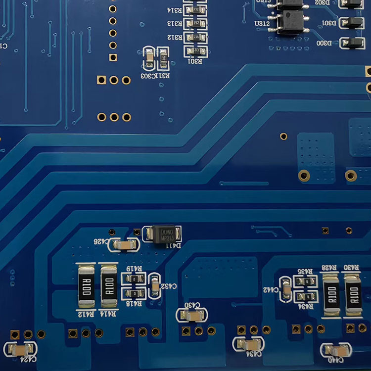
Printed Circuit Boards (PCBs) are the backbone of all modern electronics — from smartphones to satellites. But before these boards power up your favorite gadgets, they go through a detailed and highly technical process known as PCB fabrication. Whether you're a beginner or an engineer, understanding how PCBs are fabricated can give you a deeper appreciation of this critical part of electronics manufacturing.
What Is PCB Fabrication?
PCB fabrication is the process of manufacturing the physical structure of a printed circuit board. This includes creating the conductive pathways (traces), insulating layers, drilled holes, and surface finishes that together support and connect electronic components.
It is distinct from PCB assembly, which involves placing and soldering components onto the board.
Step-by-Step Process of PCB Fabrication
1. Design & Output Generation
Every PCB begins as a design, created using CAD software (like Altium Designer, Eagle, or KiCAD). The design is exported into Gerber files, which serve as blueprints for each PCB layer, including copper traces, solder masks, and silkscreens.
2. Substrate Material Preparation
The base of the PCB — usually FR4 (fiberglass-reinforced epoxy laminate) — is chosen. This material provides strength and insulation.
3. Copper Cladding
A thin layer of copper foil is laminated on one or both sides of the substrate to form the conductive layers.
4. Image Transfer & Etching
Using a photolithography process, the desired circuit pattern is transferred onto the copper layer using photoresist. The board is then etched to remove unwanted copper, leaving only the desired traces.
5. Multilayer Lamination (for multilayer PCBs)
For PCBs with multiple layers, individual layers are aligned and laminated together under heat and pressure.
6. Drilling
Tiny holes are drilled through the board using CNC machines or lasers. These holes allow for vias and component leads.
7. Plating & Via Formation
Holes are plated with copper to create electrical connections between layers (plated through-holes or vias).
8. Solder Mask Application
A solder mask is applied to protect the copper traces and prevent solder bridges during component assembly. It also gives the PCB its characteristic green (or other colored) surface.
9. Silkscreen Printing
Text, labels, logos, and component outlines are printed on the board using silkscreen ink.
10. Surface Finish
To protect the exposed copper pads and ensure solderability, a surface finish such as HASL (Hot Air Solder Leveling), ENIG (Electroless Nickel Immersion Gold), or OSP (Organic Solderability Preservative) is applied.
11. Electrical Testing
To verify the integrity of the circuits, electrical tests are performed. This includes open/short testing and continuity checks.
12. Final Inspection & Cutting
The final boards are inspected visually or via AOI (Automated Optical Inspection), then cut into shape using CNC routing or laser cutting.
Key Considerations in PCB Fabrication
Board Thickness: Influences strength and impedance.
Trace Width & Spacing: Affects current-carrying capacity and signal integrity.
Number of Layers: Determines design complexity and routing flexibility.
Tolerance & Accuracy: Critical for high-frequency or high-density boards.
Final Thoughts
PCB fabrication is a blend of engineering precision and manufacturing finesse. With growing demands for smaller, faster, and more reliable electronics, the complexity of PCBs continues to rise — and so does the importance of high-quality fabrication.