
Key points about double-layer PCB prototypes
2023-11-06
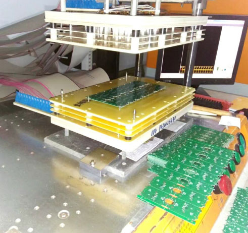
A double-layer PCB prototype refers to a printed circuit board with two layers of conductive copper traces, one on each side of the insulating substrate. These PCBs are also commonly known as 2-layer PCBs. Double-layer PCBs are widely used in electronic applications and prototypes due to their simplicity, cost-effectiveness, and versatility. Here are some key points about double-layer PCB prototypes:
1. Layer Structure: A double-layer PCB has two layers of copper traces, one on the top side and one on the bottom side. These layers are separated by an insulating substrate, typically made of materials like FR-4 (a flame-retardant epoxy laminate) or similar materials.
2. Component Mounting: Components can be mounted on both sides of the PCB, allowing for a compact design. This makes double-layer PCBs suitable for a wide range of electronic devices.
3. Prototype Development: Double-layer PCB prototypes are commonly used during the initial stages of product development. They are ideal for testing and refining circuit designs before moving on to more complex multi-layer PCBs.
4. Simplified Design: Compared to multi-layer PCBs, double-layer prototypes are generally easier to design and manufacture. This simplifies the development process and reduces costs.
5. Through-Hole Components: Double-layer PCBs can accommodate through-hole components, which are components with leads that pass through holes in the board and are soldered on both sides. This feature can be beneficial for prototyping and testing.
6. Customization: Double-layer PCB prototypes can be customized to meet the specific requirements of a project. The layout of components and traces can be tailored to the application.
7. Versatility: These prototypes can be used for a wide range of applications, including consumer electronics, automotive devices, industrial equipment, and more.
8. Manufacturing Speed: Double-layer PCB prototypes can be manufactured relatively quickly, making them a popular choice for rapid prototyping and initial testing of electronic circuits.
Double-layer PCB prototypes are an important step in the development process of electronic devices. They allow engineers and designers to validate their ideas, test circuit functionality, and identify potential issues before moving on to more complex and costly multi-layer PCBs. Once the design is verified, it can be scaled up to multi-layer PCBs for mass production if necessary.