

RFID Inlay Factory: Everything You Need to Know About Custom Manufacturing and Design
2026-05-11
Ever wondered how a simple tag transforms into a powerful tracking tool? Behind every seamless RFID inlay lies a sophisticated world of custom design and precision manufacturing. At OSRFID, that world comes to life—tailored to your exact needs. Whether you're optimizing supply chains or securing assets, understanding the inlay factory process is your first step to making it work. Ready to peek behind the curtain? Let’s dive into the essentials.
Breaking Down the RFID Inlay Manufacturing Process
RFID inlay manufacturing starts with a delicate dance of precision and material science. Thin, flexible substrates—often PET or paper—are fed through specialized machines that lay down conductive silver ink or etched aluminum into antenna patterns. The printing or etching process must maintain tight tolerances, as even micron-level deviations can affect read range and performance. After the antenna is formed, the chip is attached using anisotropic conductive adhesive, a step that requires pinpoint accuracy to ensure reliable electrical and mechanical bonding without damaging the micron-thin circuitry.
Once the chip is mounted, the assembly moves into testing and lamination. Each inlay undergoes functional checks to verify its response frequency, read distance, and memory integrity before being sandwiched between protective layers. This isn't just about slapping on a cover—the lamination material and its thickness are carefully chosen to match the intended end-use environment, whether it's a sticker for retail tags or a rugged inlay for logistics. The process blends high-speed automation with rigorous quality gates, where a single flawed inlay can be flagged and removed without slowing the entire line.
What often gets overlooked is the role of substrate preparation and environmental control. Humidity and static charges can wreak havoc during dielectric layer application, so cleanroom conditions and ionized air showers are standard. The final converting stage—cutting, scoring, and spooling—determines how easily the inlay integrates into labels or cards downstream. It's a symphony of chemistry and engineering, where every step from antenna design to final inspection shapes the little powerhouse that silently powers billions of item-level interactions every day.
Tailored Antenna Designs for Unique Applications
Every device has its own personality, and the antenna needs to match that character. Off-the-shelf solutions often force compromises in performance or aesthetics, especially when you're dealing with unusual shapes, tight spaces, or environments that would chew up a generic design. We’ve learned that the most effective approach is to listen to the product’s constraints first—its size, materials, nearby components, and the way people will actually use it—and then let those details guide the antenna’s geometry, not the other way around.
This mindset has led to creations that barely resemble traditional antennas: thin, flexible patches that disappear behind a display, laser-cut metal contours that form part of a structural bracket, or ceramic blocks that handle extreme temperatures without flinching. In one case, a wearable health monitor needed consistent connectivity while floating on a saltwater kayak; the answer involved a sealed, buoyant element that used the water itself to help shape the radiation pattern. In another, a smart farming sensor buried underground had to 'whisper' through soil—so we tuned it to embrace the very medium most designs fight against.
The beauty of tailored design is that it often uncovers hidden possibilities. Instead of fighting the enclosure or the environment, the antenna becomes an ally with those elements, sometimes even improving range or lowering power consumption by accident. It’s not about making something that works on paper but about crafting a component that genuinely fits—like a tailor altering a suit until it moves with the wearer.
Material Choices That Shape Performance and Durability
Every material we select plays a defining role in how a product behaves under real-world conditions. For structural components, high-strength alloys offer resistance to fatigue and deformation, keeping critical systems reliable even after years of heavy use. On the other hand, advanced polymers can reduce vibration and dampen noise, directly improving user comfort and precision. The art lies in matching the right material to the exact stress type and environmental exposure the part will face—there’s no universal shortcut.
Durability isn’t just about raw toughness; it’s about how a material ages. We pay close attention to oxidation resistance, ultraviolet stability, and chemical inertness, because gradual degradation often causes more failures than sudden impact. For instance, components exposed to moisture and temperature swings benefit from stainless steels with molybdenum, which fend off pitting far longer than standard grades. Similarly, we use proprietary ceramic coatings in high-wear areas to triple the surface life without adding weight.
Beyond immediate function, material selection also shapes long-term field performance in subtle ways. Thermal conductivity, for example, affects how quickly a housing dissipates heat, directly influencing internal electronics’ lifespan. Coefficient of expansion mismatches can create stress points that lead to micro-cracks over time. We prototype with multiple candidate materials, running accelerated life tests that simulate years of service in weeks, because theory alone never tells the full story. The result is a finely tuned balance of cost, weight, and endurance that sets truly reliable designs apart.
Quality Control Steps That Prevent Costly Failures
Catching defects early in the process is what separates a reliable product from an expensive recall. It starts with incoming material inspections—checking that raw components match spec sheets before they ever reach the line. If a batch of steel has micro-cracks or a circuit board supplier suddenly switches solder alloys without warning, you want to know before hundreds of units are assembled. That single checkpoint alone can save weeks of rework and prevent failures that only show up after the product reaches the customer.
In-process checks are just as critical, but they need to be designed around the way things actually get built, not some idealized flowchart. Instead of relying on end-of-line testing to catch everything, experienced teams build verification right into the assembly stations. For example, a torque sensor that locks out the next step until a bolt is tightened within tolerance, or an automated vision system that flags a misaligned gasket before the housing goes on. These inline controls don’t just catch problems—they give immediate feedback so operators can adjust, which slowly builds a culture where quality is owned by the people doing the work, not just the inspectors at the end.
Finally, a well-structured final audit isn’t about checking every unit—it’s about sampling smartly and digging into the data when something looks off. If a certain failure mode starts climbing, even slightly, that’s a signal to backtrack through the process logs and find the root cause, whether it’s a worn tool, a batch of contaminated lubricant, or a shift change that missed a critical calibration. The goal is to turn those findings into permanent changes—updated work instructions, better tooling maintenance, or supplier scorecards that carry real consequences. That’s how you stop a pattern before it becomes a field failure that costs far more than any inspection ever would.
Integrating RFID Inlays into Unconventional Products
Embedding RFID inlays into items that were never meant to carry electronics pushes the boundaries of manufacturing and design. Unlike standard labels on cardboard boxes, these inlays find their way into clothing seams, rubber tires, ceramic mugs, or event wristbands made of silicone. The challenge lies in ensuring the inlay survives the product's native forming processes—whether it's high-temperature vulcanization, injection molding, or the flexing and stretching of wearable materials. Specialized inlay designs with rugged chips and flexible antennas make this possible, turning previously untaggable objects into data carriers without altering their look or feel.
Material compatibility is at the heart of successful integration. A polycarbonate luggage shell requires an inlay that bonds during thermoforming without air bubbles or delamination, while a leather wallet demands an adhesive that won't stain or stiffen the surface. Engineers often turn to low-profile inlays with custom substrates that match the product's thermal expansion and flexibility. For textiles, robust thread-like or on-patch inlays endure washing cycles and mechanical stress. The key is treating the RFID component not as an afterthought, but as an integral part of the bill of materials from the earliest design stages.
The payoffs extend well beyond simple inventory counts. A sports equipment manufacturer can authenticate a composite hockey stick throughout its lifecycle, a brewery can track a keg's fill history even after dozens of returns, and a luxury brand can embed provenance directly into a handbag's lining. These use cases demand inlays that perform reliably on curved or metallic surfaces, often employing tuned antenna architectures that compensate for detuning effects. When done right, the technology becomes invisible to the end user yet indispensable for the supply chain, opening up entirely new service models based on continuous item-level intelligence.
What to Expect When Scaling from Prototype to Mass Production
Moving from a functional prototype to full-scale production introduces a shift in thinking that goes far beyond simply making more units. The one-off build might have relied on hand-soldered connections, 3D-printed brackets, and parts sourced from a local distributor with no thought to long-term availability. Once you commit to volume, every component has to be scrutinized for lead time, minimum order quantities, and whether the supplier can sustain quality over thousands of cycles. That custom-machined aluminum part that worked beautifully in the lab may need to be redesigned for injection molding or stamping to hit cost targets—and the redesign often spirals into cascading changes across the assembly.
Testing also takes on a completely different character. In the prototype phase, you might get away with spot-checking a handful of units, but mass production demands a rigorous, statistically driven approach. You’ll likely encounter failure modes that never appeared in the initial five builds: tolerance stack-ups that cause intermittent shorts, connector wear-out after repeated mating, or firmware glitches triggered only when a specific sensor batch is combined with a particular PCB revision. The factory environment itself becomes a variable—things like ambient humidity, operator training, and even the time of day can influence yield. Expect to invest heavily in inline inspection, automated test rigs, and a clear plan for containing and root-causing defects before they reach the customer.
FAQ
An RFID inlay is the functional core of any RFID tag, consisting of a microchip attached to an antenna on a thin substrate. The chip stores data and handles radio communication, while the antenna transmits and receives signals. A face material and adhesive backing are often added later to turn it into a finished label or sticker.
Most custom orders start with a detailed consultation to nail down the application needs, such as read range and environment. Engineers then design a prototype, which goes through a quick pilot run for testing. Once approved, the factory scales up to full production, often allowing small minimums for specialized projects.
Frequency band is the first big decision—UHF for long range or HF for near-field—along with the IC type and memory requirements. You also have to factor in the antenna size, which directly impacts read distance, and the material it’ll be attached to, since metal or liquids can detune the tag. Environmental conditions like heat, moisture, or chemicals may dictate special encapsulations.
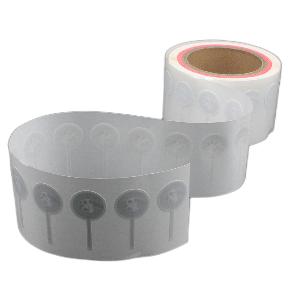
Antennas are typically made by etching copper or aluminum on a polyester carrier, or by screen printing conductive ink for lower-cost runs. Next, automated pick-and-place machines bond the RFID chips to the antenna pads with great precision. The whole web goes through an oven for curing and then gets tested roll-to-roll before being slit into individual inlays.
Absolutely. Custom die-cutting allows inlays to fit curved surfaces or tight product packaging. Flexible substrates like PET can handle repeated bending, and printable antennas open up options for odd geometries that etched metal can’t easily achieve. There are even fabric-friendly inlays for apparel that survive washing and stretching.
A solid factory runs multiple checks: inline optical inspection catches antenna defects early, while electrical testing verifies each chip’s functionality and read sensitivity. Finished inlays then face batch sampling for environmental stress—think temperature cycling and humidity exposure—to guarantee they hold up in the real world. Only rolls that pass these tests ship out.
Conclusion
Building a custom RFID inlay starts with far more than just slapping a chip onto an antenna. The manufacturing process pulls together precision etching, bonding, and lamination steps that must be tuned for the exact materials and performance targets you've set. Because every application has its own constraints—whether it's a curved medical device, a rugged logistics tag, or a fashion item that can't tolerate visible electronics—the antenna design itself often starts from scratch, shaped through iterative simulation and lab prototyping until it delivers the read range and orientation tolerance you actually need. Material choices ripple through everything: the substrate affects flexibility and heat resistance, the conductive ink or foil determines how the antenna behaves under stress, and the adhesive needs to survive the attachment method, be it sewing, overmolding, or pressure bonding in a tight space.
Once the design is locked, the real challenge is making sure every single inlay performs predictably. That means building quality gates right into the line—impedance checks, read-rate sampling, and environmental stress testing—so that a bad batch never reaches your assembly floor. When you're integrating RFID into products that weren't originally designed for it, like composite tools or wearable textiles, the conversation shifts from “will it work” to “how will it behave after 500 wash cycles or a drop onto concrete.” And scaling up from those first hand-tuned samples to full production is rarely just a numbers game. It's about balancing lead times, fine-tuning the equipment for higher throughput without losing consistency, and managing the reality that what performed beautifully in a 50-piece pilot might need subtle adjustment when you're running 50,000. A factory that truly understands custom RFID doesn't just take your order; it challenges your assumptions and helps you avoid the silent failures that show up weeks later in the field.
Contact Us
Contact Person: Esme Mo
Email: [email protected]
Tel/WhatsApp: 0086 191 2931 7837
Website: https://www.osrfidglobal.com/